 English
 Español
  Português
  русский
  Français
  日本語
日本語  Deutsch
  tiếng Việt
  Italiano
  Nederlands
  ภาษาไทย
  Polski
  한국어
한국어  Svenska
  magyar
  Malay
Malay  বাংলা ভাষার
  Dansk
Dansk  Suomi
Suomi  हिन्दी
  Pilipino
  Türkçe
  Gaeilge
  العربية
  Indonesia
  Norsk
Norsk  تمل
تمل  český
český  ελληνικά
  український
  Javanese
  فارسی
فارسی  தமிழ்
தமிழ்  తెలుగు
  नेपाली
  Burmese
  български
  ລາວ
ລາວ  Latine
  Қазақша
  Euskal
  Azərbaycan
  Slovenský jazyk
  Македонски
  Lietuvos
  Eesti Keel
  Română
  Slovenski
  मराठी
मराठी  Srpski језик

Call Us
+86-755-27806536
Email Us
add@chenghaolcm.com

What is the manufacturing process of TFT-LCD liquid crystal screen?
2022-07-28
What is the manufacturing process of TFT-LCD liquid crystal screen?
1. The manufacturing process of TFT-LCD has the following parts
①. Form a TFT array on the TFT substrate;
②. Form the color filter pattern and the ITO conductive layer on the color filter substrate;
③. Use two substrates to form a liquid crystal cell;
④. Module assembly for installing peripheral circuits and assembling backlight sources.
2. The process of forming a TFT array on a TFT substrate
4. the preparation process of the liquid crystal cell
5. Module assembly process for peripheral circuits, assembled backlights, etc.
1. The manufacturing process of TFT-LCD has the following parts
①. Form a TFT array on the TFT substrate;
②. Form the color filter pattern and the ITO conductive layer on the color filter substrate;
③. Use two substrates to form a liquid crystal cell;
④. Module assembly for installing peripheral circuits and assembling backlight sources.
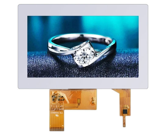
## 7.0 inch Touch Screen Module ##
2. The process of forming a TFT array on a TFT substrate
The TFT types that have been industrialized include: amorphous silicon TFT (a-Si TFT), polycrystalline silicon TFT (p-Si TFT), and single crystal silicon TFT (c-Si TFT). At present, a-Si TFT is still used.
①.First, the gate material film is sputtered on the borosilicate glass substrate, and the gate wiring pattern is formed after mask exposure, development and dry etching. A stepper exposure machine is generally used for mask exposure.
②. Continuous film formation by PECVD method to form SiNx film, non-doped a-Si film and phosphorus-doped n+a-Si film. Then, mask exposure and dry etching are performed to form the a-Si pattern of the TFT part.
③. The transparent electrode (ITO film) is formed by sputtering film formation, and then the display electrode pattern is formed by mask exposure and wet etching.
④. The contact hole pattern of the gate end insulating film is formed by mask exposure and dry etching.
⑤. Sputtering AL, etc. into a film, using a mask to expose and etch to form the source, drain and signal line patterns of the TFT. A protective insulating film is formed by the PECVD method, and then the insulating film is etched and formed by mask exposure and dry etching (the protective film is used to protect the gate, the end of the signal line electrode and the display electrode).
3. The process of forming a color filter pattern on a color filter (CF) substrate
The methods of forming the colored portion of the color filter include dye method, pigment dispersion method, printing method, electrolytic deposition method, and inkjet method. At present, the pigment dispersion method is the main method. ## 3.5 inch spi lcd display ##
The pigment dispersion method is to disperse fine pigments with uniform particles (average particle size less than 0.1 μm) (R, G, B three colors) in a transparent photosensitive resin. Then they are sequentially coated, exposed, and developed to form R.G.B three-color patterns. Photo-etching technology is used in manufacturing, and the devices used are mainly coating, exposing and developing devices.
In order to prevent light leakage, a black matrix (BM) is generally added at the junction of the RGB three colors. In the past, sputtering was often used to form a single-layer metal chromium film, but now there are also resin-type BM films that use a composite type BM film of metal chromium and chromium oxide or a resin-mixed carbon.
4. the preparation process of the liquid crystal cell
Polyimide films are respectively coated on the surfaces of the upper and lower substrates and a rubbing process is used to form alignment films that can induce molecules to be arranged as required. Then, the sealant material is distributed around the TFT array substrate, and the gasket is sprayed on the substrate.
At the same time, silver paste was coated on the transparent electrode end of the CF substrate. Then, the two substrates are aligned and bonded, so that the CF pattern and the TFT pixel pattern are aligned one by one, and then the sealing material is cured by heat treatment. When printing the sealing material, it is necessary to leave the injection port so that the liquid crystal can be pumped by vacuum. ## 4.3 inch IPS TFT Display ##
5. Module assembly process for peripheral circuits, assembled backlights, etc.
After the liquid crystal cell manufacturing process is completed, a peripheral drive circuit needs to be installed on the panel, and then polarizers are attached to the surfaces of the two substrates. If it is a transmissive LCD . Also install a backlight.
Materials and processes are the two main factors that affect product performance. TFT-LCD goes through the above four main manufacturing processes, and a large number of complicated manufacturing processes form the products we have seen.


We use cookies to offer you a better browsing experience, analyze site traffic and personalize content. By using this site, you agree to our use of cookies.
Privacy Policy
News
 Advantages of TFT Display Module2023/10/25
In real life, we all have no contact with LCD display products.
 Chenghao Display launches 8-inch Full Color Touch Display Module CH800WX02A-CTD32023/10/24
Introducing the CH800WX02A-CTD, an exceptional 8-inch full color touch display module.
Inquiry For Price List
Our sales representative will contact you within 24 hours. Thank you for your interest in our products.